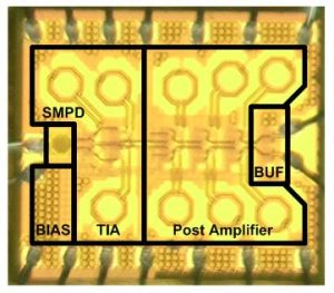
 This chip describes the design of a 10-Gb/s fully integrated CMOS optical receiver, which consists of a novel spatially-modulated photo detector (SMPD), a low-noise trans-impedance amplifier (TIA), and a post limiting amplifier on a single chip. The bandwidth of proposed meshed SMPD can be boosted up to 6.9 GHz under a reverse-biased voltage of 14.2 V. The operating speed of optical receiver is improved by 3 X compared to the prior art. To compensate the responsivity of on-chip CMOS PD, a high-gain TIA with nested feedback and shunt-peaking is proposed to achieve low-noise operation. The optical receiver is capable of delivering 25 kΩ conversion gain when driving 50 Ω output loads. Implemented in a generic 0.18-μm CMOS technology, the chip area is 0.95 mm by 0.8 mm. The input sensitivity of the optical receiver is about 18 App, and the measured responsivity of the photo detector is about 29 mA/W. Incorporating external PD with responsivity of 0.65 A/W, the input sensitivity of the optical receiver is -19 dBm for BER less than 1E-10 under 127 PRBS test pattern. The receiver core and output buffer respectively drain 118 mW and 27 mW from a single 1.8 V supply.