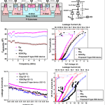
A co-packaged methodology using Transient Voltage Suppressor (TVS) chips and a controller area network (CAN) bus transceiver to ensure IEC 61000-4-2 system-level ESD protection is proposed in this work. The design methodology is verified in a high-voltage silicon-on-insulator (SOI) process for CAN transceiver chip and an 0.8-mm bipolar process for TVS chips. The I-V curves of … 閱讀全文… 關於 System-Level ESD Protection for Automotive Electronics by Co-Design of TVS and CAN Transceiver Chip
研究成果
On-Chip ESD Protection Device for High-Speed I/O Applications in CMOS Technology
The diode operated under forward-biased condition has been widely used as an on-chip electrostatic discharge (ESD) protection device for high-speed circuits to sustain high ESD robustness, but the parasitic capacitance of diode may bring a negative impact to the circuits operating at higher speed. The ESD protection design with low parasitic capacitance has been strongly … 閱讀全文… 關於 On-Chip ESD Protection Device for High-Speed I/O Applications in CMOS Technology
A Digitally Dynamic Power Supply Technique for 16-Channel 12V-Tolerant Stimulator Realized in a 0.18-μm 1.8-V/3.3-V Low-Voltage CMOS Process
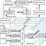
A 16-channel 12V-tolerant stimulator has been designed and successfully verified in a 0.18-μm 1.8-V/3.3-V CMOS process. It can be fully integrated with the microcontroller or the biomedical signal processor into an SoC chip fabricated in a low-voltage CMOS technology. The experimental results have shown that the proposed new digitally dynamic power supply technique for … 閱讀全文… 關於 A Digitally Dynamic Power Supply Technique for 16-Channel 12V-Tolerant Stimulator Realized in a 0.18-μm 1.8-V/3.3-V Low-Voltage CMOS Process
A Fully Integrated Closed-Loop Neuromodulation SoC with Wireless Power and Bidirectional Data Telemetry for Real-Time Human Epileptic Seizure Control
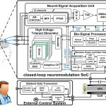
This paper presents a 16-channel closed-loop neuromodulation SoC for human seizure control. The SoC includes a 16-ch signal acquisition unit, a bio-signal processor, a 16-ch adaptive stimulator, and wireless telemetry. The signal acquisition unit amplifies and digitizes the sensed electrocorticogram (ECoG) signals. The digitized data are then processed by bio-signal processor … 閱讀全文… 關於 A Fully Integrated Closed-Loop Neuromodulation SoC with Wireless Power and Bidirectional Data Telemetry for Real-Time Human Epileptic Seizure Control
A 81-dB Dynamic Range 16-MHz Bandwidth DS Modulator Using Background Calibration
A fourth-order discrete-time delta-sigma modulator (DSM) was fabricated using a 65-nm CMOS technology. It combines low-complexity circuits and digital calibrations to achieve high speed and high performance. The DSM is a cascade of two second-order loops. It has a sampling rate of 1.1 GHz and an input bandwidth of 16.67 MHz with an oversampling ratio of 33. It uses high-speed … 閱讀全文… 關於 A 81-dB Dynamic Range 16-MHz Bandwidth DS Modulator Using Background Calibration